HaLow Ink
A pocket node for Heltec's HT-HC01 Wi-Fi HaLow module: an ESP32-S3 drives the radio and a 2.9-inch e-paper screen, and a LiPo charged over USB-C runs it for months between reports. It speaks ordinary IP to a HaLow access point a kilometre or more away. Everything on this page was generated from one design file and checked by KiCad; none of it has been built yet.
Designed and rule-checked · not yet fabricated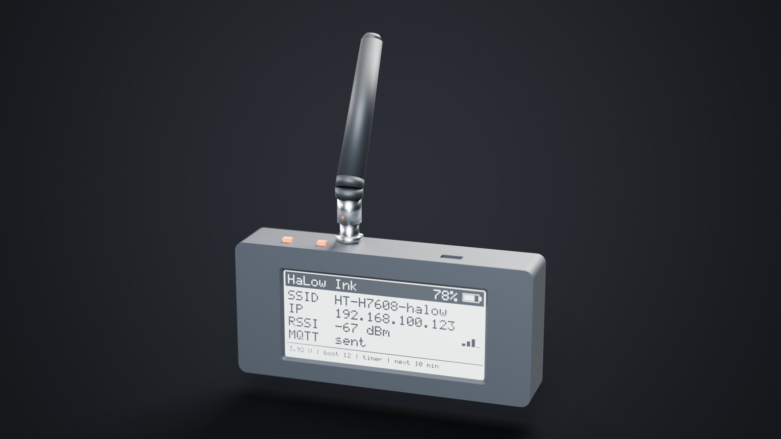
Renders
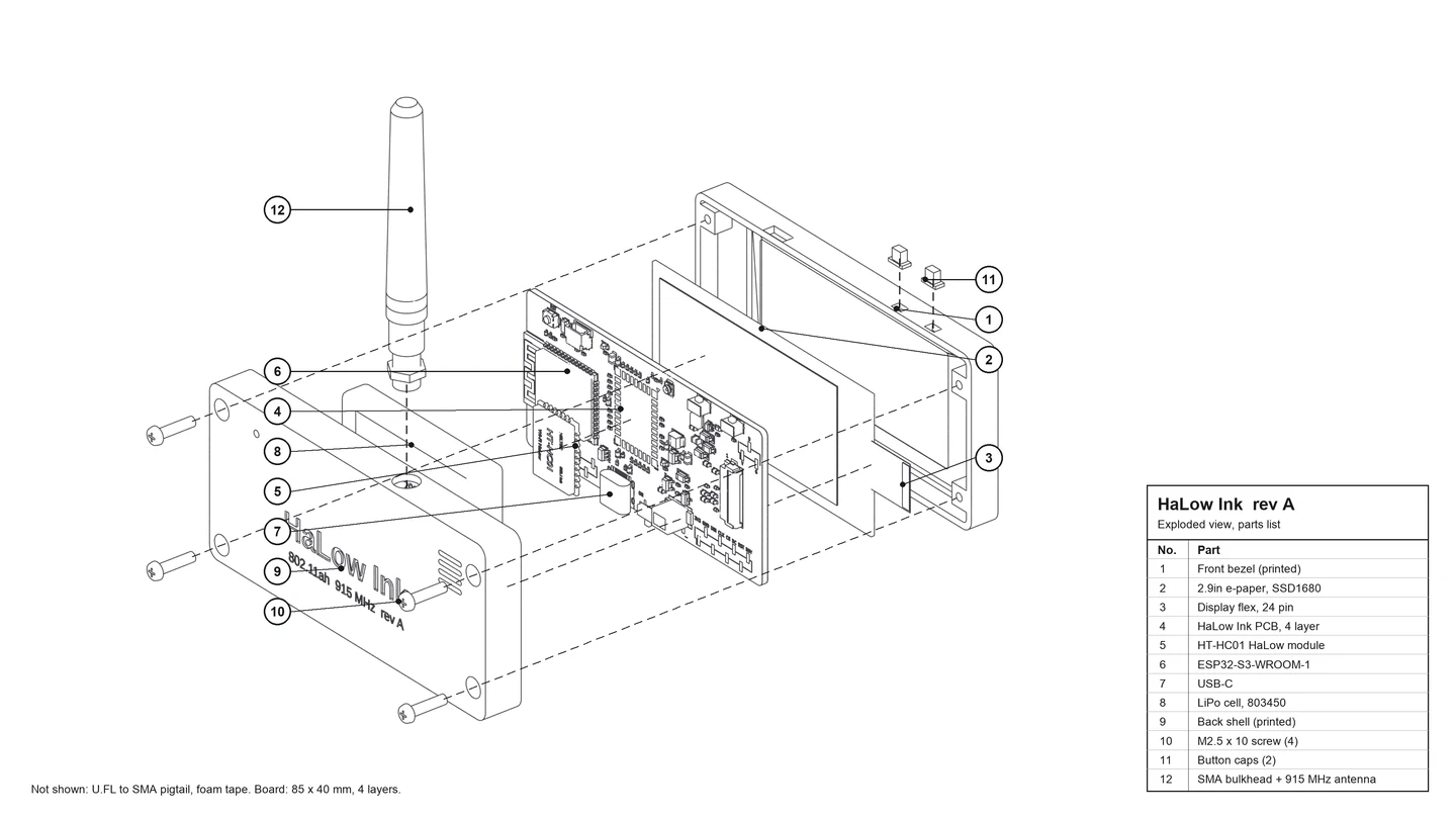
Blender Cycles, 3840 × 2160. The board comes straight out of KiCad. The HT-HC01, the display, the cell, the screws and the antenna were modelled from their datasheets, and the case from its OpenSCAD source. Click any picture for the full size.
Walk around it
The same assembly as the renders, slimmed down for a browser. Drag to turn it, scroll or pinch to zoom, and pull the slider to take it apart. Print parts switches to the three STL files as they sit on the printer's bed.
How it is wired
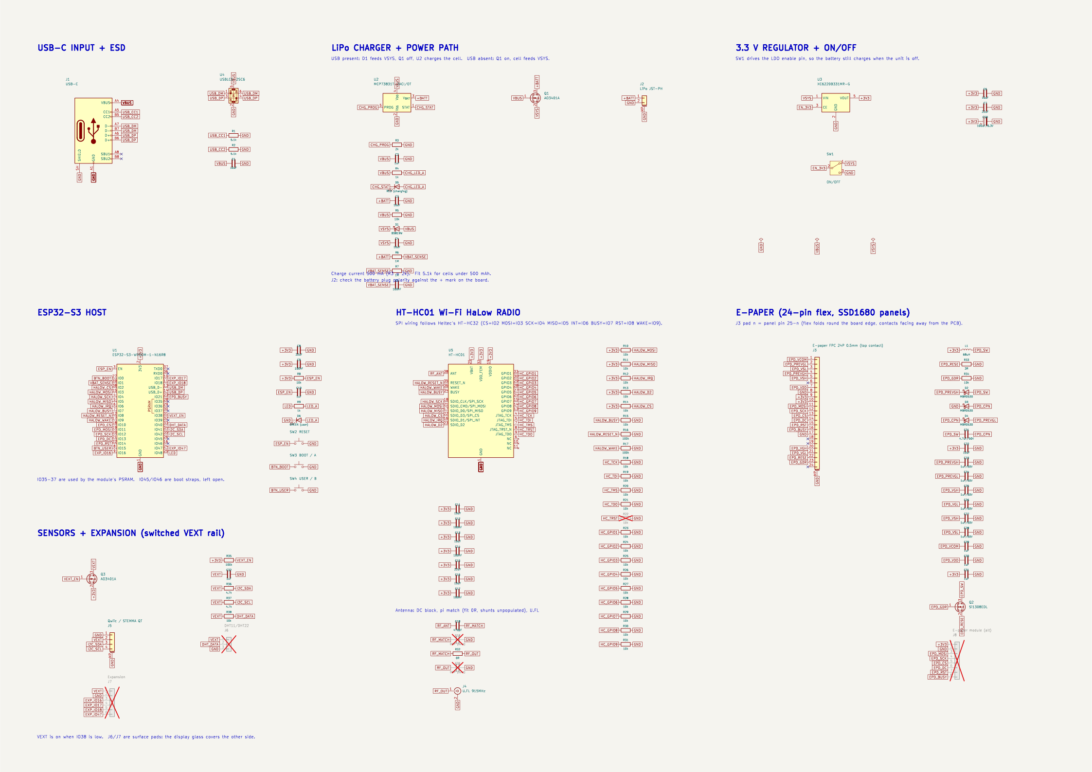
The HT-HC01 is a radio only, so the ESP32-S3 runs it over SPI at up to 40 MHz through the module's SDIO pads. The pins match Heltec's own HT-HC32 board, so their Arduino core and Morse Micro's ESP-IDF component need no changes to find the radio.
| Function | ESP32-S3 | Notes |
|---|---|---|
| HaLow SPI CS / MOSI / SCK / MISO | IO2 / 3 / 4 / 5 | HC01 pads 22 / 21 / 18 / 17 |
| HaLow interrupt | IO6 | pad 16, active low |
| HaLow BUSY / RESET_N / WAKE | IO7 / 8 / 9 | RESET_N and WAKE pulled low: the radio waits for firmware |
| E-paper CS / MOSI / SCK / DC / RST / BUSY | IO10 / 11 / 12 / 13 / 14 / 21 | its own SPI bus |
| Battery voltage | IO1 | 1M / 1M divider |
| Buttons A / B | IO0 / IO15 | both wake it from deep sleep |
| Qwiic SDA / SCL | IO41 / IO42 | 4.7k pull-ups on the switched rail |
| DHT data · sensor rail · LED | IO40 · IO38 · IO48 | rail on when IO38 is low |
| Spare pads | IO16 / 17 / 18 / 47 | GPS, buzzer, anything |
| USB | IO19 / IO20 | native USB, no serial chip |
Power path
USB feeds the regulator through a Schottky diode and charges the cell through an MCP73831 at 500 mA. Unplugged, a P-channel FET connects the cell instead. The slide switch drives the regulator's enable pin, so the cell still charges with the unit off.
Radio supply
The HT-HC01's three supply pads each get their own 10 µF and 100 nF, the amplifier's pad another 22 µF, and a 100 µF tantalum sits on the 3.3 V rail for transmit bursts of about 220 mA.
Schematic
Four layers, 85 × 40 mm
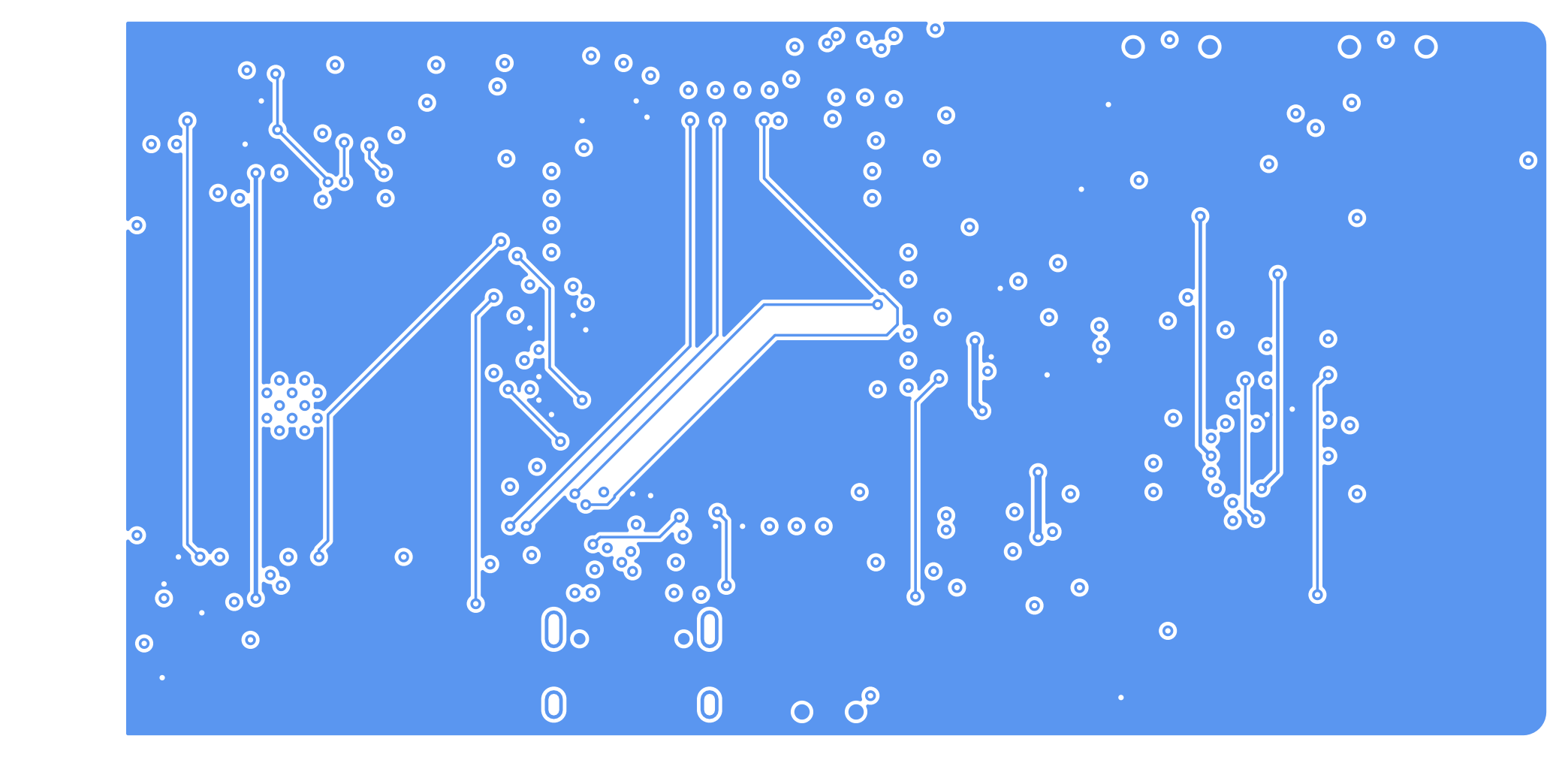
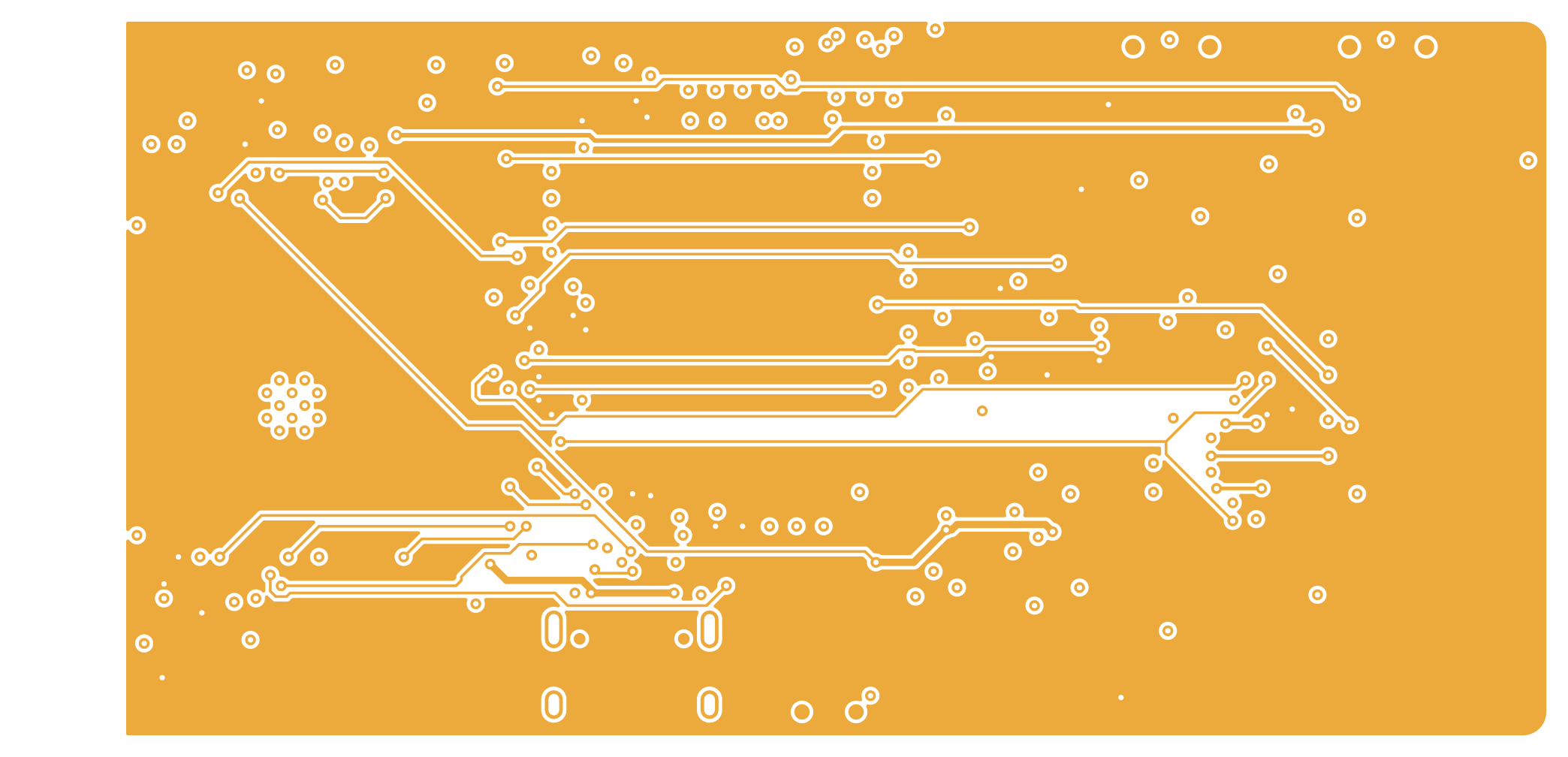
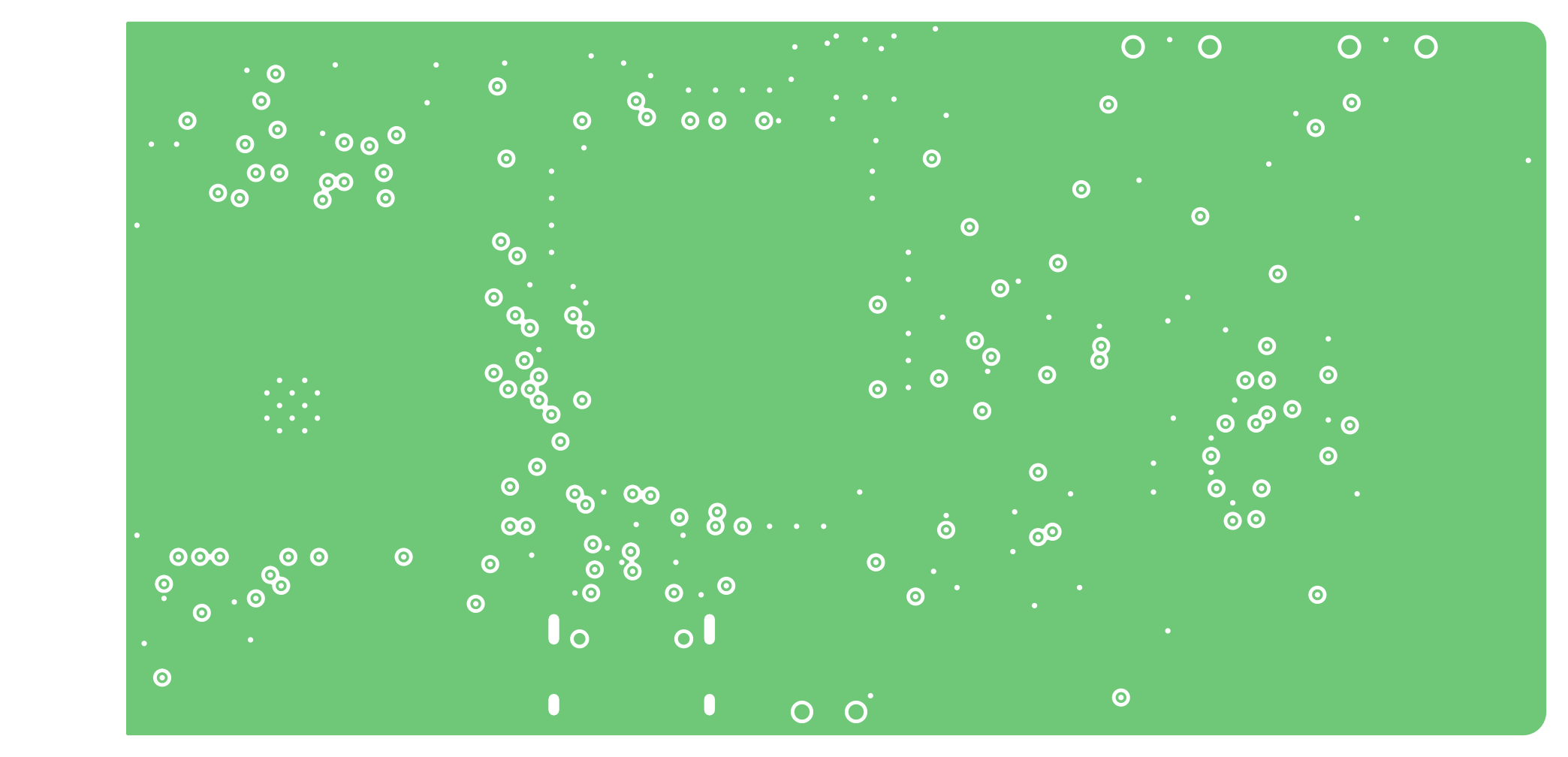
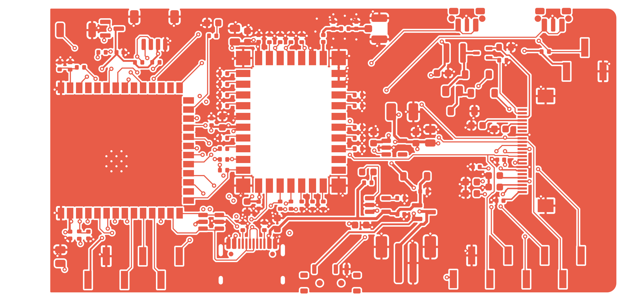
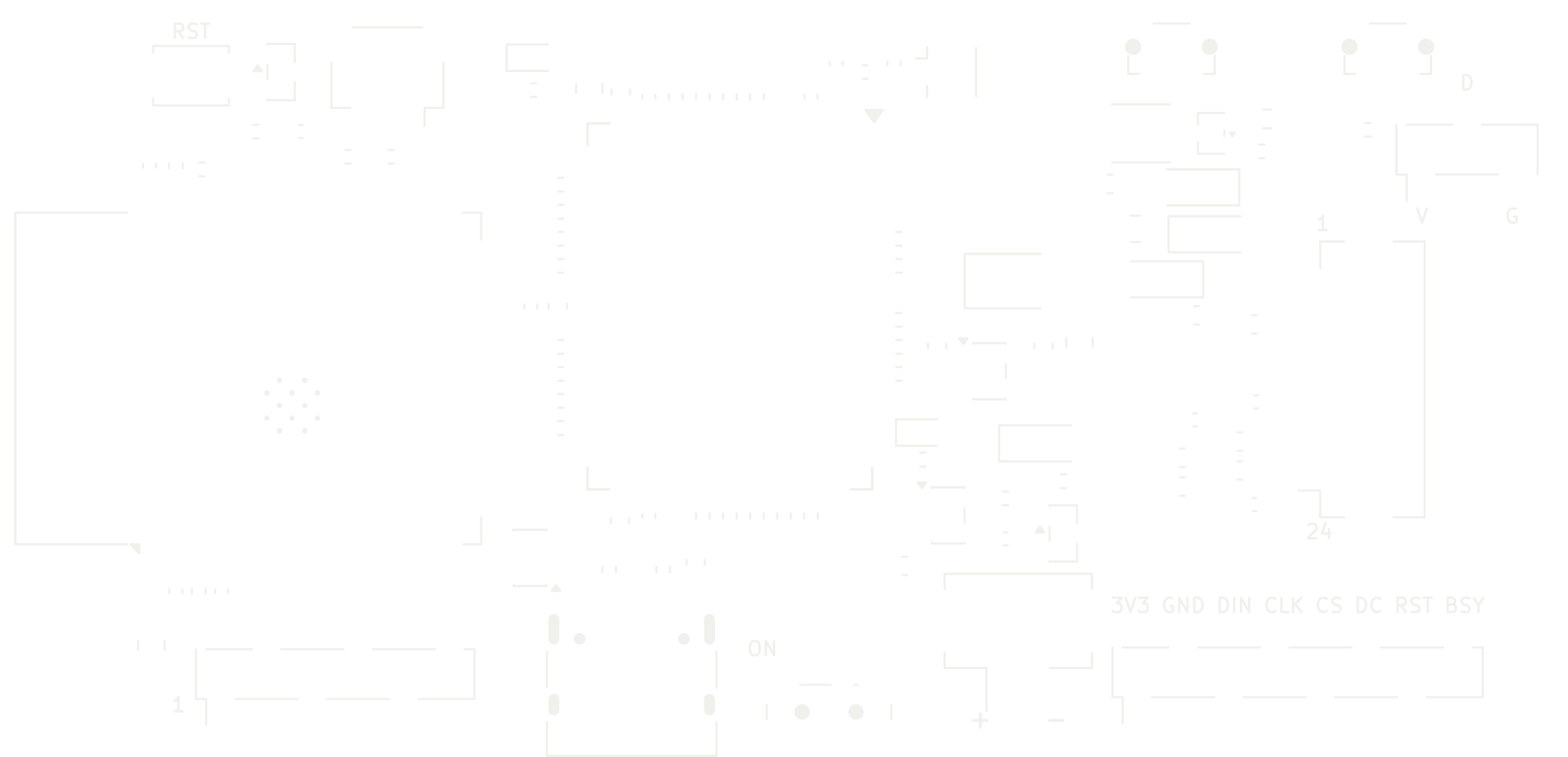
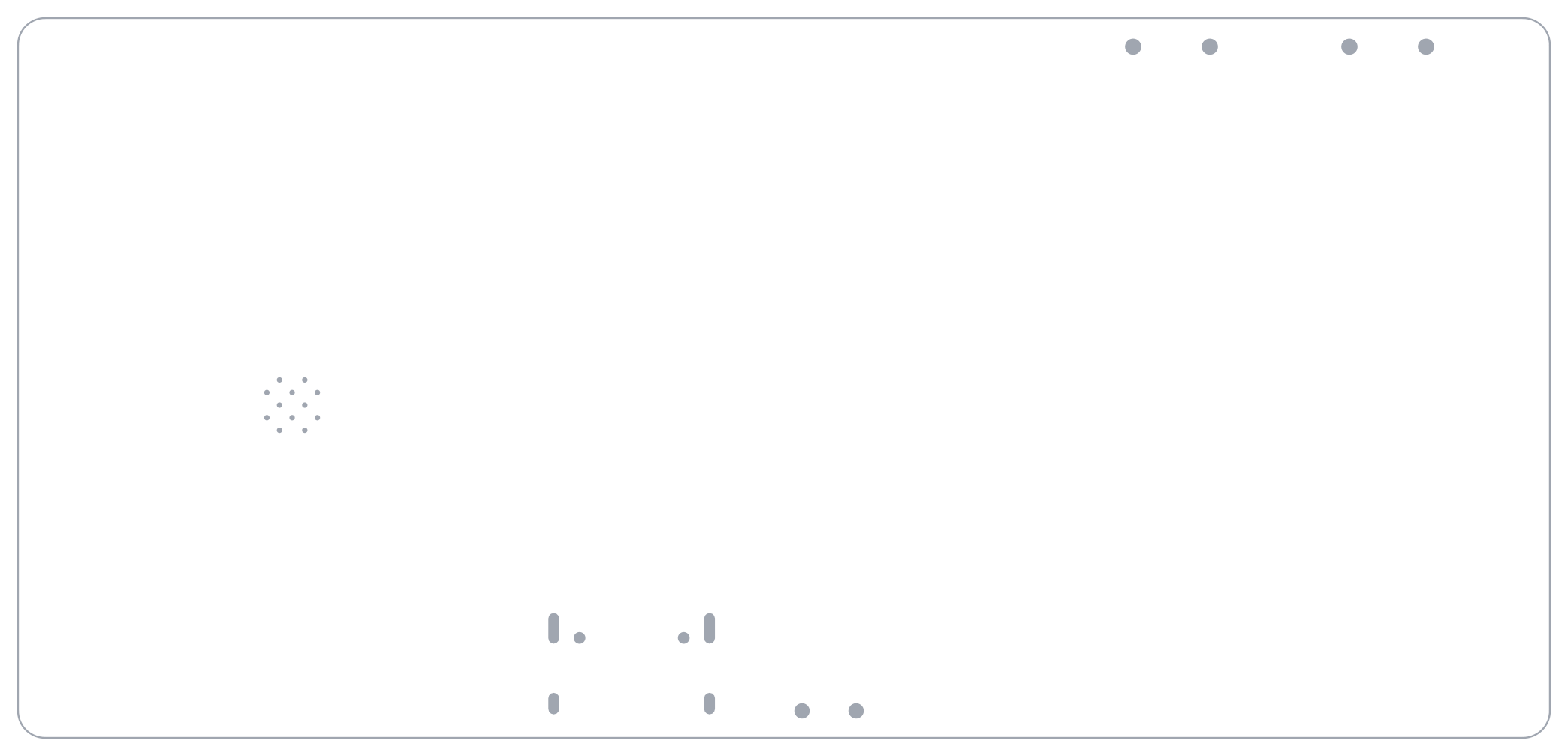
Front copper carries the parts and short hook-ups. Inner 1 is solid ground. Inner 2 takes east–west signals and a 3.3 V pour, and the back takes north–south signals and a second 3.3 V pour. Nothing runs on top under either radio module, and the ESP32's antenna end has no copper at all. Turn layers on and off below.
Where the battery goes
HaLow draws real current only while it is awake. The radio's own figures, from Heltec's HT-HC01 datasheet at 3.3 V (VBAT plus the amplifier rail, 1 MHz channel), on a log scale:
| How it is used (whole board, estimated, not measured) | Average | 2000 mAh lasts |
|---|---|---|
| Asleep between reports: ESP32 deep sleep, regulator, divider, leakage | 20–30 µA | years, if it never woke |
| Sensor node, one report every 10 minutes | ≈ 12 mAh / day | ≈ 5 months |
| Always reachable: radio in power save, ESP32 in light sleep | ≈ 1 mA | 2–3 months |
| Radio held awake, listening | ≈ 40 mA | ≈ 2 days |
Bill of materials
36 different parts and 91 placements for JLCPCB to fit: 18 basic parts and 18 extended. All were in stock on 2026-11-13, and they come to about $10.22 a board at single-unit prices. The HT-HC01 is yours to solder by hand.
| Qty | Refs | Value | Part number | LCSC | Fitted by | Stock | Each |
|---|---|---|---|---|---|---|---|
| 8 | C1 C3 C4 C6 C11 C13 C16 C22 | 10uF | CL10A106KP8NNNC | C19702 | JLCPCB basic | 11,710,215 | $0.0233 |
| 6 | C2 C10 C29 C30 C31 C32 | 1uF | CL05A105KA5NQNC | C52923 | JLCPCB basic | 10,438,873 | $0.0057 |
| 5 | C5 C9 C12 C14 C17 | 100nF | CL05B104KO5NNNC | C1525 | JLCPCB basic | 31,892,084 | $0.0024 |
| 3 | C7 C8 C15 | 22uF | CL21A226MAQNNNE | C45783 | JLCPCB basic | 4,182,833 | $0.1084 |
| 1 | C18 | 470pF | 0402B471K500NT | C1537 | JLCPCB extended | 344,742 | $0.0027 |
| 2 | C19 C20 | DNP (tune) | not fitted | ||||
| 1 | C21 | 4.7uF/50V | CL21A475KBQNNNE | C98192 | JLCPCB extended | 132,202 | $0.0447 |
| 6 | C23 C24 C25 C26 C27 C28 | 1uF/50V | CL10A105KB8NNNC | C15849 | JLCPCB basic | 13,422,278 | $0.0083 |
| 1 | C50 | 100uF/6.3V | TAJB107K006RNJ | C16133 | JLCPCB basic | 574,952 | $0.2515 |
| 1 | D1 | B5819W | B5819W | C8598 | JLCPCB basic | 359,341 | $0.0262 |
| 3 | D2 D3 D4 | MBR0530 | MBR0530T1G | C82046 | JLCPCB extended | 202,017 | $0.0629 |
| 1 | D5 | RED (charging) | KT-0603R | C2286 | JLCPCB basic | 5,864,318 | $0.0077 |
| 1 | D6 | GREEN (user) | 19-217/GHC-YR1S2/6T | C2986059 | JLCPCB extended | 406,269 | $0.0171 |
| 1 | J1 | USB-C | TYPE-C-31-M-12 | C165948 | JLCPCB extended | 536,848 | $0.1869 |
| 1 | J2 | LiPo JST-PH | B2B-PH-SM4-TB(LF)(SN) | C160352 | JLCPCB extended | 68,428 | $0.2050 |
| 1 | J3 | E-paper FPC 24P 0.5mm (top contact) | FH12A-24S-0.5SH(55) | C506794 | JLCPCB extended | 1,602 | $0.8262 |
| 1 | J4 | U.FL 915MHz | U.FL-R-SMT-1(80) | C88374 | JLCPCB extended | 294,824 | $0.1092 |
| 1 | J5 | Qwiic / STEMMA QT | SM04B-SRSS-TB(LF)(SN) | C160404 | JLCPCB extended | 6,501 | $0.2147 |
| 1 | J6 | DHT11/DHT22 | not fitted | ||||
| 1 | J7 | Expansion | not fitted | ||||
| 1 | J8 | E-paper module (alt) | not fitted | ||||
| 1 | L1 | 68uH | FNR3015S680MT | C167769 | JLCPCB extended | 10,030 | $0.0460 |
| 2 | Q1 Q3 | AO3401A | AO3401A | C15127 | JLCPCB basic | 1,548,364 | $0.0814 |
| 1 | Q2 | Si1308EDL | SI1308EDL-T1-GE3 | C469327 | JLCPCB extended | 39,647 | $0.2602 |
| 2 | R1 R2 | 5.1k | 0402WGF5101TCE | C25905 | JLCPCB basic | 3,963,119 | $0.0014 |
| 1 | R3 | 2k | 0402WGF2001TCE | C4109 | JLCPCB basic | 10,048,426 | $0.0019 |
| 2 | R4 R9 | 1k | 0402WGF1001TCE | C11702 | JLCPCB basic | 31,561,762 | $0.0013 |
| 23 | R5 R8 R10 R11 R12 R13 R14 R15 R18 R19 R20 R21 R23 R24 R25 R26 R27 R28 R29 R30 R31 R34 R38 | 10k | 0402WGF1002TCE | C25744 | JLCPCB basic | 21,210,598 | $0.0010 |
| 2 | R6 R7 | 1M | 0402WGF1004TCE | C26083 | JLCPCB basic | 2,359,423 | $0.0012 |
| 3 | R16 R17 R35 | 100k | 0402WGF1003TCE | C25741 | JLCPCB basic | 8,491,230 | $0.0011 |
| 1 | R22 | 10k | 0402WGF1002TCE | not fitted | |||
| 1 | R32 | 0R | 0402WGF0000TCE | C17168 | JLCPCB basic | 15,740,652 | $0.0012 |
| 1 | R33 | 3R | 0603WAF300KT5E | C23157 | JLCPCB extended | 26,483 | $0.0033 |
| 2 | R36 R37 | 4.7k | 0402WGF4701TCE | C25900 | JLCPCB basic | 14,323,762 | $0.0017 |
| 1 | SW1 | ON/OFF | MSK12C02 | C431540 | JLCPCB extended | 172,338 | $0.0544 |
| 1 | SW2 | RESET | TS-1088-AR02016 | C720477 | JLCPCB basic | 916,144 | $0.0516 |
| 1 | SW3 | BOOT / A | SKRTLAE010 | C110293 | JLCPCB extended | 43,632 | $0.1435 |
| 1 | SW4 | USER / B | SKRTLAE010 | C110293 | JLCPCB extended | 43,632 | $0.1435 |
| 1 | U1 | ESP32-S3-WROOM-1-N16R8 | ESP32-S3-WROOM-1-N16R8 | C2913202 | JLCPCB extended | 21,983 | $5.3481 |
| 1 | U2 | MCP73831T-2ACI/OT | MCP73831T-2ACI/OT | C424093 | JLCPCB extended | 8,835 | $0.7902 |
| 1 | U3 | XC6220B331MR-G | XC6220B331MR-G | C86534 | JLCPCB extended | 10,464 | $0.4761 |
| 1 | U4 | USBLC6-2SC6 | USBLC6-2SC6 | C7519 | JLCPCB extended | 42,522 | $0.1569 |
| 1 | U5 | HT-HC01 | HT-HC01 | you, by hand |
Not on the board order
- HT-HC01 (V1, 21 dBm), hand-soldered.
- 2.9″ 296 × 128 e-paper with the SSD1680 24-pin flex (Waveshare 2.9″ V2 raw panel, Good Display GDEY029T94).
- LiPo with a JST-PH lead, 34 × 50 mm, 6 to 10 mm thick. Check its polarity first.
- 915 MHz antenna and a U.FL-to-SMA bulkhead pigtail.
- Four M2.5 × 10 screws.
Putting one together
- Order the board.Upload the Gerbers to JLCPCB: 4 layers, 1.6 mm, stack-up JLC04161H-7628. Turn on top-side assembly with the BOM and placement files, then check every polarised part in their placement preview.
- Solder the HT-HC01.There is about 1 mm of bare board beside every pad for the iron. Check that the antenna pad has not bridged to the ground pads on either side.
- Bring it up on USB.No battery and no display yet. Check for 3.3 V, then flash the firmware over the USB-C port.
- Fit the display.Tape the glass to the back of the board inside the corner marks. Fold the flex round the board's end and into the connector, contacts away from the board. The silkscreen marks pin 1.
- Connect the cell.Meter the plug against the board's + and − marks first. There is no reverse-polarity protection.
- Close the case.The board drops into the bezel display-first. Put the cell on foam tape over the two modules, fit the SMA bulkhead and clip the pigtail to the U.FL. Drop in the button caps and fit the four screws.
What it does when it wakes
An ESP-IDF project using Morse Micro's HaLow component. It builds; it has never run on hardware.
- Wake.Timer, button A, button B or power-on. It reads the battery before the radio draws current.
- Boot the radio.Morse Micro's library loads the MM6108's firmware and the HT-HC01's board configuration file over SPI.
- Join.It associates with the access point (an HT-H7608 here) and waits for a DHCP lease, 30 s at most.
- Report.It publishes one JSON status message over MQTT at QoS 1 and waits for the broker's acknowledgement.
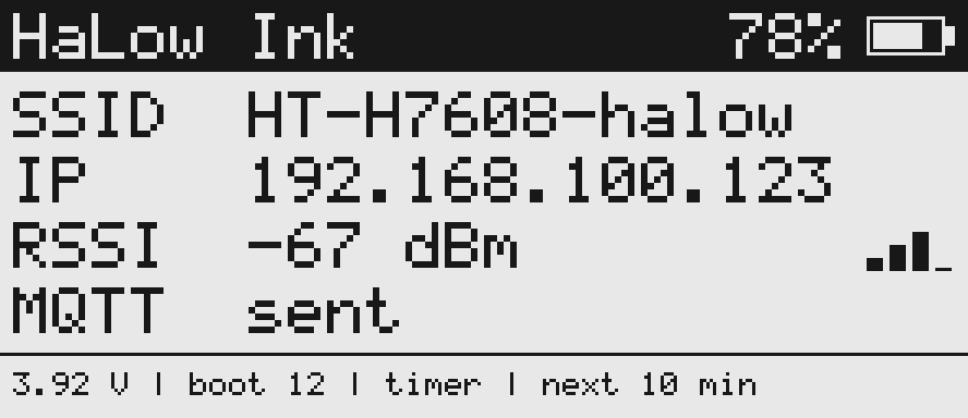
- Draw.It shuts the radio down, then redraws the screen: SSID, address, RSSI, MQTT result, battery and wake reason.
- Sleep.Deep sleep for 10 minutes, with the radio held in reset. A watchdog forces sleep if anything hangs.
Wi-Fi HaLow, briefly
Ninety seconds on what Wi-Fi HaLow is, how far it reaches, what it costs in data rate and power, and where HaLow Ink fits. Narrated by a cartoon of me in my cloned voice; every figure on screen names its source.
Before you order
- Display flex orientation. Worked out from Waveshare's drawing, with a top-contact connector (Hirose FH12A). Hold a real panel against the board before buying.
- Part rotation at JLCPCB. The placement file is KiCad's raw output. Check the SOT-23s, diodes, LEDs, the tantalum, the ESP32 and the connectors in their preview.
- Battery polarity. JST-PH LiPo leads are not wired the same way by every vendor, and there is no reverse protection.
- Antenna path. 0 Ω link and two empty shunt positions, as in Heltec's reference design. Not simulated or measured.
- Automatic routing. It passes every rule check, but no layout engineer has reviewed it.
- The case is a first draft. Print one and check the buttons, the USB opening and the window before trusting the dimensions.